Memory
Non-Volatile memory
Retains data on power off
Read-Only Memory(ROM)

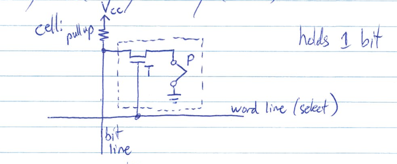
- P~connection: closed = 0, open = 1, read by setting transistor T's gate high which closes connection
- contents programmed at foundry via mask
- mask cost is high => large production runs necessary
Programmable ROM(PROM)
- P is a fuse
- blow fuse with high V to write '1'
- can only write once
- mobile phones, RFID tags
Erasable PROM(EPROM)
- P is a special transistor that traps charge(for decades)
- erased by ultraviolet light(through quartz window)
- (erased = zero or one? TODO ask)
Electrically Erasable PROM(EEPROM)
- different voltages for writing, reading and erasing
- any byte can be writte
- multiple writes
- aka NVRAM
Flash
- like EEPROM but erased/written in block
- cheaper than EEPROM
- used in LPC1678, USB memory sticks, cameras
Volatile Memory
Loses data on power-off
Static RAM(SRAM)

- write by driving bit line b and its complement b'
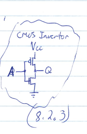
- fast(invertors actively drive bit lines)
- large area(6 transistors) => expensive
- used for cache memory

Dynamic RAM(DRAM)

- C: charged=1, discharged=0
- write by driving bit line to Vcc or ground
- read: pre-charge bit line to Vgnc < V < Vcc, sense(amplify) signal, write back(reading 1 discharges C)
- about 4x slower than SRAM
- Periodic refresh(T=~10ms)
- small area => cheaper
- used for main memory
Classification
| Type |
Volatile? |
Writable |
Erase Size |
| ROM |
no |
no |
- |
| PROM |
no |
once |
- |
| EPROM |
no |
yes |
whole chip |
| EEPROM |
no |
yes |
byte |
| Flash |
no |
yes |
block |
| SRAM |
yes |
yes |
byte |
| DRAM |
yes |
yes |
byte |
Memory Chips
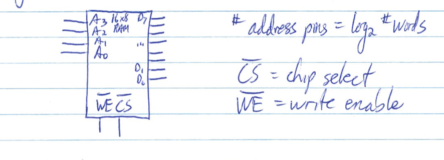
e.g. 16 word x 8 bit chip

For internal view, see handout
Decoder asserts a word line to enable a raw
Large Memory Chips
e.g. 2M word x 8 bit (221 words)
requires 21 x 2097152 decoder(slow!)
instead, arrange bit cells in symmetric array
221 words x 23 bits/word
= 224 bits(16M)
= 212 x 212 bits
= 4096 x 4096 bits
see handout
decoder is 12 x 4096
each row contains 4096/8 = 512 words
need 512:1 mux to select word
put address bits A20 - A9 on pins and assert Row Address Strobe(RAS) to select row
next put A8 - A0 on pins and assert Column Address Strobe(CAS) to select word
timing diagram: async DRAM read(2 words)

Fast Page Mode
- add latch to sense/write circuit that holds entire row
- only have to select RAM once if addresses from same row
- timing diagram: async DRAM FPM read(2 words)
- DRAM controlled asynchonously by timing RAS and CAS
- common until mid-90s
Synchronous DRAM(SDRAM)
- control circuit integrated into memory
- programmed for bursts of 1, 2, 4, 8, ... words
- timing diagram: SDRAM read(2 -word burst)
- takes starting address and produces words in consecutive bus cycles(from same row)
Double Data Rate(DDR) SDRAM
- data transferred as rising and falling edge of bus cycle
- timing diagram: SDRAM DDR read(2-word burst)
-
memory has to "banks" timed to different clock edges and data is stripped across banks
-
|0| |1|
- |2| |3|
-
...
-
DDR: 2000, DDR2: 2003, DDR3: 2007, DDR4: 2013
- same principle just faster circuitry
- naming convention: PC{2, 3, 4} - b/w b/w = #MB/s
e.g. PC3-12800 - 800MHz clock
=> 1600MT/s x 8 bytes/transfer = 12 800MB/s
Metrics
- latency: delay from start until first word produced(e.g. 5 cycles)
- bandwidth: volume of data per unit time
e.g. word size = 8 bytes, clock speed = 200MHz, 2 word read
Hz = cycle / s
Async: 2 words x 8 bytes / word x 200 MHz / 12 cycles = 267 MB/s
FPM: 16 bytes x 200MHz / 9 cycles = 356 MBs
SDRAM: 16 bytes x 200MHz / 7 cycles = 457 MB/s
DDR: 16 bytes x 200MHz / 6 cycles = 533 MB/s
Modules
- DIMM: dual inline memory module
- multiple memory chips on a PCB(printed circuit board)
- e.g. 1GB / DIMM with 64M word x 8 bit chips

- 2 sides(bank), 8 chips / side
- volume = 64 MB / chip x 8 chip / side x 2 sides = 512 MB/side x 2 sides = 1GB
- dual-channel = 2 DIMMS side by side => 128 bits in parallel
Click here for the next chapter
